
ICs Packaging
- Home
- /
- POSTS
- /
- Technology
- /
- ICs Packaging
The integrated circuit chip is too small and delicate to be handled directly. Each chip is bonded to a set of tiny gold or aluminum wires and set into a flat block of plastic or ceramic. The block has metal pins on the outside, leading to the wires inside. The pins form a solid mechanical and electrical connection to other components in a system.
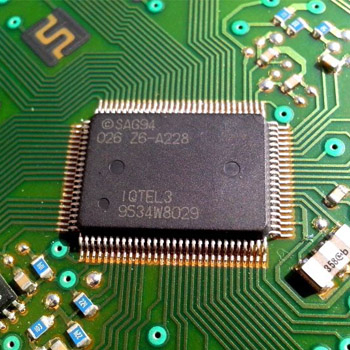
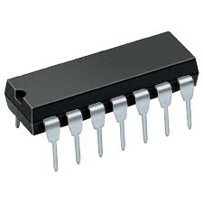
Ics come in a variety of package types. Simple chips come in a dual-inline package, or dip. These are long rectangles with four, seven, eight, or more pins on either side. As chip complexity has grown, designers have added more pins. Some microprocessor chips have hundreds of pins. These are arranged in neat rows on the bottom of the chip.
The frequently used analog ic is an operational amplifier or simply called as an op-amp, similar to the differential amplifier, but possesses a very high voltage gain. It consists of very less number of transistors compared to the digital ics, and, for developing analog application specific integrated circuits (analog asics), computerized simulation tools are used. The plastic block protects the ic chip and helps keep it cool.
The manufacturer name and part number is usually printed on the top.
The integrated circuits that are obtained by the combination of analog and digital ics on a single chip are called as mixed ics.
These ics functions as digital to analog converters, analog to digital converters (d/a and a/d converters) and clock/timing ics. The circuit depicted in the above figure is an example of mixed integrated circuit which is a photograph of the 8 to 18 ghz self healing radar receiver.
Ic design can be divided into the broad categories of digital and analog ic design. Digital ic design is to produce components such as microprocessors, fpgas, memories (ram, rom, and flash) and digital asics. Digital design focuses on logical correctness, maximizing circuit density, and placing circuits so that clock and timing signals are routed efficiently. Analog ic design also has specializations in power ic design and rf ic design.
Analog ic design is used in the design of op-amps, linear regulators, phase locked loops, oscillators and active filters.
Analog design is more concerned with the physics of the semiconductor devices such as gain, matching, power dissipation, and resistance. Fidelity of analog signal amplification and filtering is usually critical and as a result, analog ics use larger area active devices than digital designs and are usually less dense in circuitry.
An integrated circuit or monolithic integrated circuit (also referred to as an ic, a chip, or a microchip) is a set of electronic circuits on one small flat piece (or “Chip”) of semiconductor material, normally silicon. The integration of large numbers of tiny transistors into a small chip resulted in circuits that are orders of magnitude smaller, cheaper, and faster than those constructed of discrete electronic components.
The ic’s mass production capability, reliability and building-block approach to circuit design ensured the rapid adoption of standardized ics in place of designs using discrete transistors.
Ics are now used in virtually all electronic equipment and have revolutionized the world of electronics. Computers, mobile phones, and other digital home appliances are now inextricable parts of the structure of modern societies, made possible by the small size and low cost of ics.
Ics were made possible by experimental discoveries showing that semiconductor devices could perform the functions of vacuum tubes, and by mid-20th-century technology advancements in semiconductor device fabrication. Since their origins in the 1960s, the size, speed, and capacity of chips have progressed enormously, driven by technical advances that allow more and more transistors on chips of the same size – a modern chip may have several billion transistors in an area the size of a human fingernail.


