
EPC-Space Radiation-Hardened Gallium Nitride (Rad-Hard GaN)

- Home
- /
- POSTS
- /
- Technology
- /
- EPC-Space Radiation-Hardened Gallium Nitride...
Radiation-hardened electronics, referred to as RadHard, are electronic components that are designed and produced to be immune to the damaging exposure of radiation and extreme temperatures found in rugged environments, such as space.
Unlike silicon-based technology, where special processing is required to protect the semiconductor against the total ionizing dose (TID) of the effects of radiation, the physical properties and construction of gallium nitride (GaN) devices make it relatively immune to the damage caused by such radiation in space.
Regarding Single Event Effects (SEE), both silicon and GaN require special processing to be immune.
There are three primary types of radiation that devices in orbit are subject to: gamma radiation, neutron radiation and heavy ion bombardment.
Gamma Radiation – eGaN Transistors

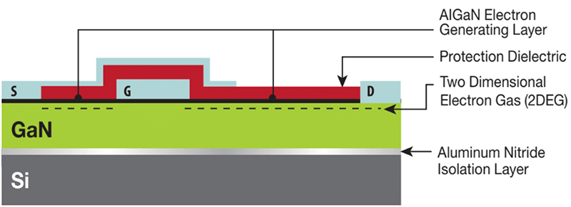
In enhancement mode GaN (eGaN®) devices, all three terminals; gate, source, and drain, are located on the top surface. Like in a silicon MOSFET, conduction between source and drain is modulated by biasing the gate electrode from zero volts to a positive voltage – usually 5 V.
In the eGaN device, the gate is separated from the underlying channel by an aluminum gallium nitride layer. This layer does not accumulate charge when subjected to gamma radiation and therefore GaN devices do not experience the charge ‘trapping’ effect that silicon MOSFETs do when exposed to gamma radiation.
Neutron Radiation – eGaN Transistors
As with gamma radiation, the impact of neutrons on the GaN crystal and the entire device structure is minimal. The reason for GaN’s superior performance under neutron radiation is that GaN has a much higher displacement threshold energy compared with silicon.
Heavy Ion Bombardment (SEE) – eGaN Transistors
Single Event Effects (SEE) are caused by highly energetic heavy ions and protons/neutrons impinging on sensitive areas within the transistor. Since eGaN devices do not have a gate oxide, they are immune to single event gate rupture (SEGR).
Because eGaN FETs do not have the parasitic bipolar junctions that exist within MOSFETs, they are also not prone to single event upset (SEU) or single event burnout (SEB).
GaN devices can however be impacted by heavy ion bombardment, which manifests as a slow degradation in drain-source leakage as the heavy ion fluence increases. Using special processing and design, eGaN devices can be made as immune to SEE as they are inherently immune to TID.
Read Full article on EPC Space Rad Hard GaN
MICROREL – Via Guido Rossa 34, CP.00065 – Fiano Romano, ROME, ITALY
Phone : +39 334 9529414
Email1: d.lauta@protec-semi.com
Email2: danilo.lauta@microrel.com
Web: www.microrel.comIn Partnership with:
Rosenheimer Landstraße 117, D-85521 Ottobrunn-Riemerling, Germany
Phone: +49 (0)89 6602923
Email: sales@protec-semi.de
Web: www.protec-semi.de
CONTACT MODULE


