
MMIC Design
- Home
- /
- POSTS
- /
- RF Microwave
- /
- MMIC Design
A Monolithic Microwave Integrated Circuit, or MMIC is a type of integrated circuit (IC) device that operates at microwave frequencies (300 MHz to 300 GHz) and fabricated using gallium arsenide (GaAs), a III-V compound semiconductor.
These devices typically perform functions such as microwave mixing, power amplification, low-noise amplification, and high-frequency switching. Inputs and outputs on MMIC devices are frequently matched to a characteristic impedance of 50 ohms.
MMICs are dimensionally small (from around 1 mm² to 10 mm²) and can be mass-produced, which has allowed the proliferation of high-frequency devices such as cellular phones.
It has two fundamental advantages over silicon (Si), the traditional material for IC realisation: device (transistor) speed and a semi-insulating substrate. Both factors help with the design of high-frequency circuit functions. However, the speed of Si-based technologies has gradually increased as transistor feature sizes have reduced, and MMICs can now also be fabricated in Si technology. The primary advantage of Si technology is its lower fabrication cost compared with GaAs.
Silicon wafer diameters are larger (typically 8″ to 15″ compared with 4″ to 8″ for GaAs) and the wafer costs are lower, contributing to a less expensive IC.
Originally, MMICs used MEtal-Semiconductor Field-Effect Transistors (MESFETs) as the active device. More recently High Electron Mobility Transistors (HEMTs), Pseudomorphic HEMTs (PHEMT) and Heterojunction Bipolar Transistors (HBT) have become common.
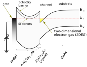 A High-electron-mobility transistor (HEMT) is a field-effect transistor (FET) incorporating a junction between two materials with different band gaps (i.e. a heterojunction) as the channel instead of a doped region (as is generally the case for MOSFET). Like other FETs, HEMTs are used in integrated circuits as digital on-off switches.
FETs can also be used as amplifiers for large amounts of current using a small voltage as a control signal. Both of these uses are made possible by the FET’s unique current-voltage characteristics. HEMT transistors are able to operate at higher frequencies than ordinary transistors, up to millimeter wave frequencies, and are used in high-frequency products such as cell phones, satellite television receivers, voltage converters, and radar equipment. They are widely used in satellite receivers, in low power amplifiers and in the defense industry.
The heterojunction bipolar transistor (HBT) is a type of bipolar junction transistor (BJT) which uses differing semiconductor materials for the emitter and base regions, creating a heterojunction. The HBT improves on the BJT is that it can handle signals of very high frequencies, up to several hundred GHz. It is commonly used in modern ultrafast circuits, mostly radio-frequency (RF) systems, and in applications requiring a high power efficiency, such as RF power amplifiers in cellular phones.
Other III-V technologies, such as indium phosphide (InP), have been shown to offer superior performance to GaAs in terms of gain, higher cutoff frequency, and low noise. However they also tend to be more expensive due to smaller wafer sizes and increased material fragility.
Silicon germanium (SiGe) is a Si-based compound semiconductor technology offering higher-speed transistors than conventional Si devices but with similar cost advantages.
 Gallium nitride (GaN) is also an option for MMICs.
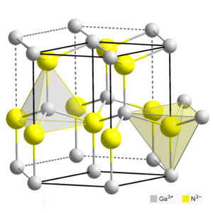
Because GaN transistors can operate at much higher temperatures and work at much higher voltages than GaAs transistors, they make ideal power amplifiers at microwave frequencies. Gallium nitride (GaN) is a binary III/V direct bandgap semiconductor commonly used in light-emitting diodes. The compound is a very hard material that has a Wurtzite crystal structure.
In addition, GaN offers promising characteristics for THz devices.


